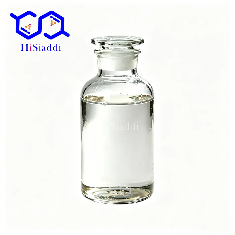

HiSiaddi is an innovative foreign trade service provider driven by dual pillars of technology commercialization and foreign trade services. We have established a service system structured as "1+2+3+4=1" and can supply original factory materials of well-known brands for triethylene glycol divinyl ether. As a foreign trader with independent R&D capabilities, HiSiaddi has repeatedly resolved customized product demands for triethylene glycol divinyl ether through technological cooperation with manufacturers and precise insight into market demands. Below is a case detailing how we addressed customized requirements for triethylene glycol divinyl ether.
Please contact HiSiaddi customer service if you require more customized service solutions.
OPTICOAT OY from Finland, a listed fine optoelectronic materials enterprise headquartered in Helsinki with 31 years of expertise in R&D and manufacturing of high-end semiconductor photolithography supporting monomers, UV-curable optical resins and liquid crystal intermediates. Its products are mass-supplied to Nordic chip wafer fabs and leading manufacturers of high-end optical films, complying with EU REACH, CLP, semiconductor raw material IEC cleanliness standards, control of REACH Substances of Very High Concern (SVHC), and Finnish chemical environmental access regulations.
Triethylene glycol divinyl ether (TEGDVE) serves as the core raw material for the client’s deep-UV photolithography diluent monomers and high-transmittance optical UV resins. Raw material quality directly impacts the photoresist’s light transmittance, curing shrinkage rate and storage stability. The client has sourced high-purity original grades from Japan’s Showa Denko for years with a stable annual customized procurement volume of 115 tons.
In the past two years, Japanese raw material prices have surged continuously, sea freight lead times have extended to 70 days, and customized production capacity of overseas major manufacturers has been restricted. Expansions by wafer clients have further tightened raw material supply, prompting the Finnish firm to launch localized Chinese alternative customization. The client independently contacted 4 domestic ether fine chemical manufacturers for sample trial production, yet all multi-round tests over 3 months ended in failure.
Most domestic manufacturers mass-produce general industrial-grade triethylene glycol ethers with fixed catalytic and rectification production lines, and are unwilling to retrofit equipment or conduct refined impurity removal for niche high-end optoelectronic raw materials. Conventional industrial products contain dozens of times the allowable levels of aldehyde, alcohol and vinyl residual impurities, failing to meet photolithography material standards and halting the client’s pilot production of new photoresists. The client fully entrusted HiSiaddi with end-to-end customized services including indicator decomposition, factory screening, process customization, three-stage pilot testing and export compliance management.
1. Purity of main component triethylene glycol divinyl ether ≥99.75%; total content of monoether and diether isomer impurities ≤200ppm
2. Residual raw material triethylene glycol ≤50ppm, acetaldehyde ≤10ppm, vinyl alcohol by-products ≤15ppm (common domestic industrial products contain over 3000ppm of these three impurities)
3. Water content ≤30ppm, color APHA ≤5 (colorless and transparent; trace colored impurities cause a sharp drop in UV transmittance of photoresists)
4. Polymerization inhibitor content precisely controlled at 8–12ppm: excessive inhibitor impairs photosensitivity, while insufficient inhibitor leads to spontaneous polymerization and deterioration during storage
5. Single metal ion content (Na, Fe, K, Ca) ≤5ppb; metallic impurities cause local exposure defects on wafers during photolithography
6. Packaging: clean-grade iron drums lined with internal coated stainless steel; full nitrogen-sealed protection during filling. Each batch is accompanied by complete GC/HPLC impurity chromatograms, stability test reports, English pharmacopoeia-grade Certificates of Analysis (COA), and full sets of EU-compliant Safety Data Sheets (SDS).
Most domestic ether producers adopt strong alkali catalysis and conventional batch single-tower rectification processes, with production lines dedicated to mass manufacturing of general ether diluents for coatings. Retrofitting catalytic systems, adding multi-stage precision vacuum rectification and low-temperature closed inhibitor dosing units incurs high equipment renovation and R&D costs. Given the low proportion of niche high-end optoelectronic raw material orders in manufacturers’ overall capacity, factories lack incentive to adjust production lines for customized photolithography-grade products.
Alcohols, aldehydes and isomeric by-products generated during synthesis have similar boiling points. Conventional atmospheric rectification can only remove high-boiling heavy components, making it difficult to strip trace low-boiling aldehyde and alcohol impurities—the key bottleneck preventing compliance with photolithography-grade standards. Factories lack supporting refined adsorption purification sections and dedicated molecular sieve selective impurity removal equipment.
Vinyl ether products are highly prone to spontaneous polymerization. Industrial products are mass-dosed with high concentrations of inhibitors, while photolithography materials require an extremely narrow dosing window for inhibitors. Minor deviations directly compromise end photosensitive performance. Manufacturers lack low-temperature closed micro continuous dosing equipment, leading to excessive batch-to-batch fluctuations in inhibitor content during mass production.
Domestic manufacturers can only provide simple national standard quality inspection certificates, without full SVHC screening conducted in accordance with EU optoelectronic raw material requirements or 6-month long-term storage stability tests. Specialized test reports for photolithography raw materials are unavailable, preventing customs clearance and warehouse entry even if sample physicochemical indicators meet standards.
Drawing on domestic vinyl ether industrial chain resources, HiSiaddi screened 2 fine chemical manufacturers out of 13 ether producers equipped with DMC catalytic units, multi-stage continuous vacuum rectification lines and precision physical & chemical laboratories. We collaborated with the manufacturers’ R&D centers to conduct targeted technical retrofits aligned with client specifications:
1. Deploy selective composite catalytic systems to reduce generation of alcohol and aldehyde by-products during reaction, controlling impurity formation at the source
2. Build an independent four-stage stepped precision vacuum rectification dedicated line to cut fractions accurately by segment, paired with specialized molecular sieve adsorption towers for deep removal of trace low-boiling aldehyde and alcohol impurities, stabilizing total miscellaneous impurities within 140–190ppm
3. Maintain full nitrogen sealing and low-temperature temperature control in finished product buffer tanks, with inhibitor continuously and precisely metered via micro dosing pumps and real-time online sampling testing to stabilize inhibitor content at 9–11ppm, satisfying narrow-range control standards
1. Lab-scale trial (8kg samples): Finalize basic synthesis and rectification parameters; submit samples to authoritative third-party domestic optoelectronic material laboratories for full-indicator testing. Upon qualification, small drums are air-shipped to Finland. The client conducts lab-scale photoresist synthesis to test transmittance and curing sensitivity, with rectification collection temperature and inhibitor ratios fine-tuned based on finished product data.
2. Medium-scale trial (600kg continuous batches): Run 3 parallel consecutive medium-scale production batches. Retain samples from each batch for 6-month room-temperature light-shielded accelerated stability tests to identify risks of color change, purity degradation and spontaneous polymerization during storage, and formalize standardized mass production SOP process documents.
3. Mass production trial order (15 tons): HiSiaddi deploys dedicated process engineers to reside on-site for full-process central control inspections, conducting sampling and testing at every stage from raw material feeding, synthetic reaction, multi-stage rectification, refined impurity removal to closed filling to strictly control indicator fluctuations.
1. Uniformly adopt semiconductor raw material-specific 200L iron drums lined with stainless steel; drums undergo nitrogen purging to remove water and oxygen prior to filling to eliminate impurities introduced by packaging materials.
2. HiSiaddi collaborates with factory quality inspection teams to compile full technical archives: full-component chromatographic impurity spectra, three-batch long-term stability reports, SGS-SVHC 253-item full screening reports; prepare English-Finnish bilingual SDS and EP-format English COA in compliance with EU CLP and REACH regulations. The complete document set satisfies both Finnish customs clearance and semiconductor manufacturer warehouse entry audits.
Reserve dedicated customized line capacity with manufacturers for phased production aligned with the client’s monthly consumption plans. Coordinate dangerous goods customs brokers to complete UN classification, dangerous goods declaration and commodity inspection clearance, matching shipping schedules for on-time delivery to Finland.
1. The 15-ton trial order successfully cleared Finnish customs. The client utilized the material for photoresist manufacturing, with finished product transmittance, curing shrinkage and storage stability fully matching Showa Denko’s original Japanese products. Wafer photolithography defect rates were equivalent to imported materials, enabling full integration into mass production lines.
2. Comprehensive procurement costs for localized customized raw materials decreased by 32.6% compared to Japanese imports, completely resolving the client’s raw material shortage and price inflation issues. A 115-ton annual phased procurement framework was formally signed (30 tons Q1, 32 tons Q2, 28 tons Q3, 25 tons Q4).
3. The client fully entrusted HiSiaddi with targeted development and customization of two new generations of ultra-high-precision photolithography monomer raw materials the following year, alongside expanded cooperative procurement of modified vinyl ethers for supporting UV resins.
1. Domestic fine ether chemical manufacturers focus on mass production of general coating-grade products. High-precision niche raw materials for optoelectronics and semiconductors are difficult to customize independently by manufacturers when dealing directly with overseas clients due to high technical retrofit costs and low single-product capacity share.
2. Core value of HiSiaddi: A complete industrial chain service loop linking end optoelectronic indicator decomposition, factory process retrofitting, multi-gradient trial production, third-party specialized testing and full EU compliance, bridging technical, regulatory and process gaps between upstream manufacturers and high-end overseas optoelectronic clients.
3. Procurement logic for mid-to-high-end European and American semiconductor & optoelectronic materials: Precise trace impurity control, batch stability and complete compliant traceability documentation take priority over unit price. Technical supporting services represent the core competitive advantage for realizing domestic substitution and securing long-term client partnerships.
Please contact HiSiaddi customer service if you require more customized service solutions.

 +86-13120989737
  info@hisiaddi.com
 English